1.1 Computer organization
The logic diagrams in this section are made with CircuitMaker Student V6.2c by Protel Technology, Inc.
1.1.1 Logic gates
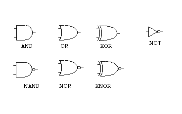
Logic gates are pretty self-explanatory once you understand what they are all about. All inputs to and outputs from a logic gate are thought of as either true or false (denoted T/F, or 0/1, or high/low).
But let's take a couple of examples.
The AND-gate takes two (or more) inputs, which all can be either true or false (1 or 0 / high or low), as just explained. Let's say we have the simplest of AND-gates, with only two inputs. For this AND-gate to output T, both inputs most be T. This is reflected in its name. Is both input A and B true? If yes, then output is true. If one input is false, then the output is false. If both inputs are false, then output is false.
OR, on the other hand, only demands that one of the inputs are true in order for the output to be true. Is A OR B true? If yes, one of them is (or both are) true, then A OR B is true, and the output is true.
XOR (exclusive or) is the same as OR, with the exception that both inputs cannot be true (if they are, output is false). So, if A OR B is true, but not both, then A XOR B is true.
The NOT-gate simply inverts its input. Hence, if input is true, then output is false, and vice versa.
The NAND-gate is and AND-gate with an inverter after it. Likewise, the NOR- and XNOR-gates are OR- and XOR-gates with inverters after them. The circle you can see on all these gates denotes the negation (the NOT, so to speak).
You can see truth-tables for AND and OR-gates in the Boolean algebras-pages, and in the logic-pages. The two pages uses slightly different notations. In Boolean algebra, OR is often written as +, and AND as *. In logic, OR is Ú and AND is Ù. This might sound confusing, but you should get the hang of it, it really isn't difficult.
The convince yourself of the logic, you should draw truth-tables for all the gates. (Do it! Do it! Do it! Do it!)
1.1.2 Alternative logic-gate representations
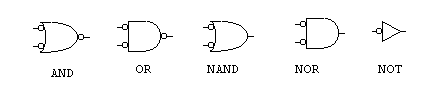
Let's take the AND-gate as an example. If you look at the picture of an OR-gate in section 1.1.1, you will find that the AND-gate you se here, is very much like that OR-gate, but now with three inverters (NOTs) on it. And you would be perfectly right. What is going on here? Well, remember that the AND-gate only outputs true if both its inputs are true.
Let's draw the truth-table for this new AND-gate. A and B are the inputs. A means NOT A (hence if A is true, A is false, and vice versa), B means NOT B, X means NOT X, and this NOT X is what this gate outputs.
| A | B | A | B | X = A or B | X |
| F | F | T | T | T | F |
| F | T | T | F | T | F |
| T | F | F | T | T | F |
| T | T | F | F | F | T |
We see from the table that only when A AND B are both true, is the output true, and this was what we wanted an AND-gate to do, right?
1.1.3 Memory (Flip-flops)
Main source: Tocci
The gates we have seen so far only rely on their immediate inputs for their outputs. But what if we want a circuit with memory? The most important memory circuit is a flip-flop (FF). The most basic FFs can be constructed from either two NAND gates or two NOR gates.
The NAND gate latch (latch)
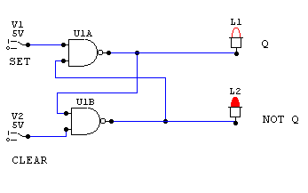
In its initial resting state, with both set and clear resting at 1 (true), the output of this latch is equally likely to be Q=1 as Q=0. But when it is set or cleared, it stabilizes and remembers its state.
To set the latch, simply turn SET = 0 (and then turn it back to 1). This will cause Q to be 1 (true) until CLEAR is set to 0 (remember to set CLEAR back to 1 again). This, in turn will set Q = 0, and it will keep being 0 until SET is set to 0 again.
The NOR FF is similar, but with Q and NOT Q reversed.
Clock signals and clocked flip-flops
Clocked J-K flip-flop
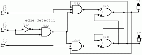
V1 = J, V3 = K, V2 = CLK, U3A and U3B is the pulse steering circuit, and U4A and U4B is a NAND-latch. L1 is Q, and L2 is Q.
If J=K=1, then a clock pulse will make Q and Q alter their states.
Clocked SC flip-flop
![]()